Microlenses and Their Optical Qualities: Size, Fabrication, and Applications in the Industry
Microlenses represent unique optical components renowned for their miniature size and exceptional light-manipulating abilities. They stand out due to their ability to focus and manipulate light at a microscopic level, enabling high-resolution imaging and precise light control.
How Small are Microlenses?
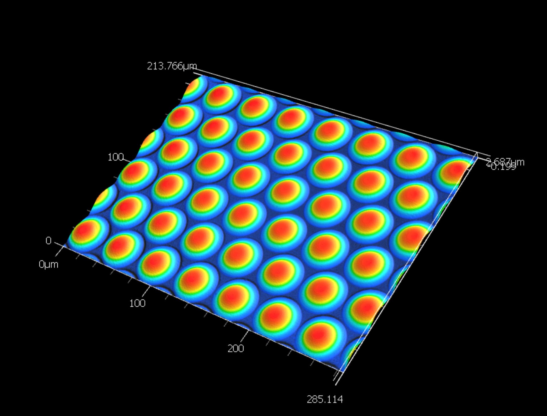
Microlenses typically possess diameters in the range of tens of micrometers, making them marvels of miniaturization. Their small size facilitates good optical quality through simple design; however, optical diffraction may introduce unwanted effects.
Traditionally, microlenses feature a single element with one plane surface and one spherical convex surface, allowing skillful refraction of light. However, advancements in microlens technology have led to more sophisticated designs incorporating aspherical surfaces and multiple layers of optical material.
Fabrication Processes: How to Fabricate Microlenses
Various fabrication techniques play a role in producing microlens arrays, depending on desired specifications. These techniques encompass photolithography, replica molding, direct laser writing, and hot embossing.

Photolithography
This technique involves depositing a light-sensitive material onto a substrate, exposing it through a patterned mask, and then removing the uncured material to leave behind the desired microlens shape.
Replica Molding
A master microlens is prepared beforehand, and a mold is created by replicating the master microlens using materials such as epoxy or PDMS. Multiple replicas can then be produced using the mold.
Direct Laser Writing
A focused laser beam is used to selectively solidify a photosensitive material, allowing for precise control over the creation of complex microlens arrays.
Hot Embossing
Utilizing a focused laser beam, this method selectively solidifies a photosensitive material, enabling precise control over the creation of complex microlens arrays.
Applications of Microlenses
With this method, a prepared mold with a microlens shape undergoes heating and pressing against a thermoplastic material, causing it to deform and take on the shape of the mold. This method proves cost-effective for large-scale production.

Imaging and Optics
They are crucial for achieving higher resolutions and clearer images in imaging systems such as digital cameras and microscopes.
Displays and Projection Systems
Microlenses enhance brightness, contrast, and viewing angles in display technologies.
Fiber Optics and Telecommunication
They improve the coupling efficiency between fibers and optoelectronic devices in communication systems.
Biomedical
Additionally, microlenses enhance imaging capabilities in microscopes and endoscopes, as well as improve efficiency in laser-based medical surgeries.
Microfluidics and Lab-On-Chip Devices
Furthermore, microlenses are employed for the manipulation and analysis of tiny fluid droplets. They can also be used to focus and direct laser beams for microfluidic control, as well as to improve detection sensitivity in miniaturized analytical devices.
Solar Energy
They contribute to the improvement of the optical efficiency of solar panels by focusing sunlight onto photovoltaic cells.
High-Security Features
In addition, microlenses are utilized in diffractive optical security features on official documents such as banknotes and passports.
Automotive
There are plenty of applications in the automotive industry. Starting from safety sensors that can be precisely adjusted to perform for a long time, to improving the quality and resolution of images captured by cameras in the front and back of vehicles.
Summary
In summary, microlenses, with their miniature size and exceptional optical properties, play a pivotal role in various technological applications. The evolution of microlens technology has led to innovative fabrication techniques, enabling the production of intricate designs and complex structures. As we continue to integrate microlenses into diverse applications, their impact on efficiency, precision, and performance remains undeniable.

Leave a comment