Micro & Nanofabrication: Engineering Structures
The fabrication of a structure is not only the first, but a crucial step in a long production chain that determines the quality and efficiency of the final product. Engineering structures involve choosing an adequate manufacturing process using the most cost-effective technology for each unique case. At 3D AG, we believe that micro and nanofabrication is a key element in achieving success. However, we also recognize that it is essential to align this step with the entire production process to ensure maximum efficiency and optimal results.
Micro and Nanofabrication: Unlocking the Future
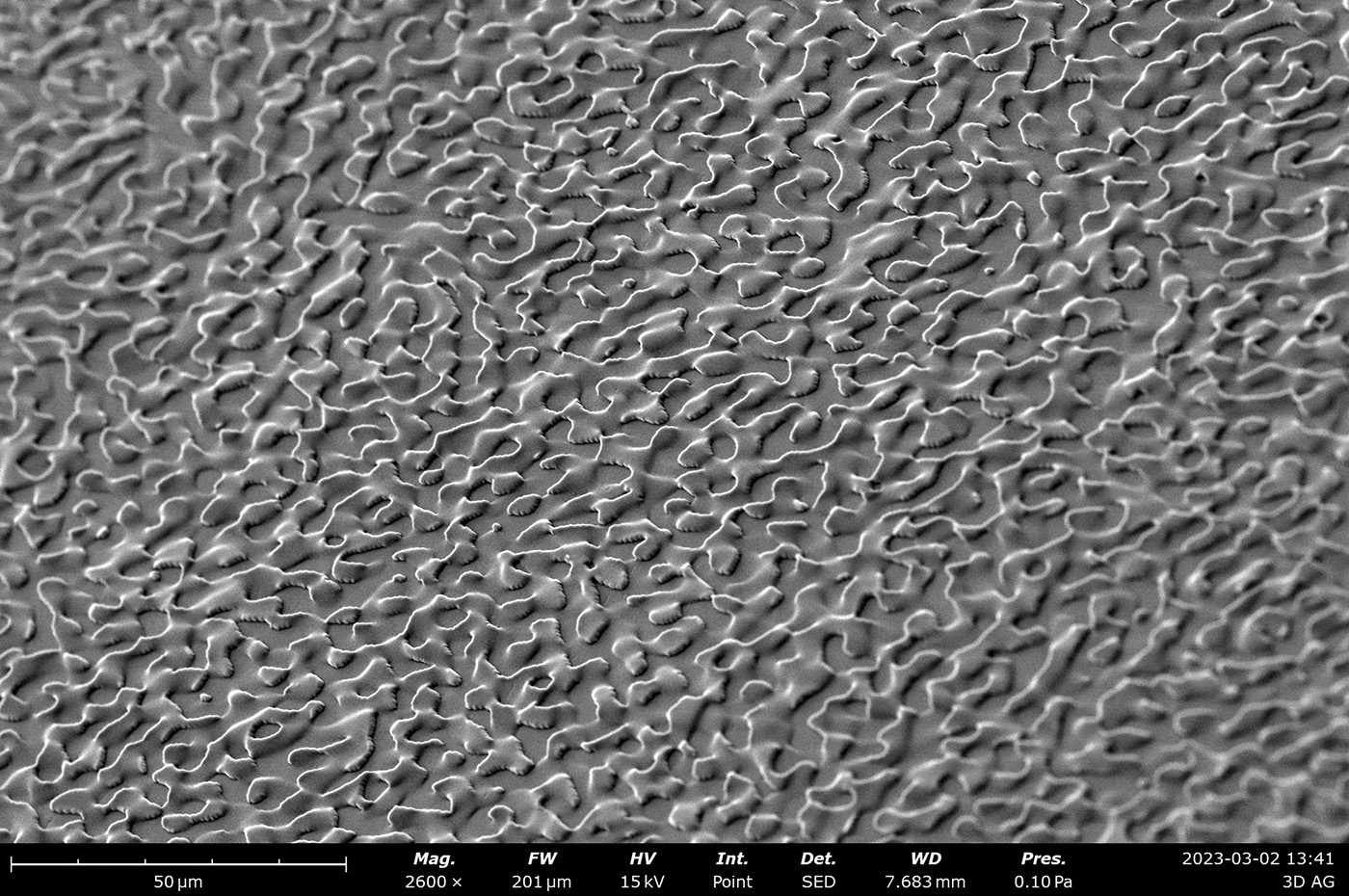
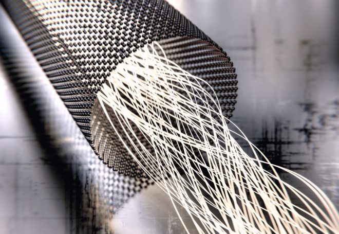
Microfabrication and nanofabrication are the basis of manufacturing many products used in our daily life. From computer chips and sensors, to screens, cars, phones, medical devices, security features and more – we are surrounded by micro and nanostructures in nature and integrated in products as visual or functional surfaces. In response to the growing complexity of demand, extensive research and development of new technologies for micro and nanofabrication techniques have revolutionized many industries. The development of complex and multifunctional products usually consists of various materials and technologies. Most recent research is focused within the nanometer scale. Results delivered by nanopatterning and products with nanostructured materials show unique electrical, magnetic, optical and thermal properties and superior performance.
3D AG has specialized in supporting the development of micro or nanostructured materials – from the idea into a manufacturable solution. With this we want to unlock the future of industries such as biology, medicine, high security and photonics.
Micro & Nanostructured Materials
3D AG has gained a lot of experience in mastering and nanopatterning and we will support you in defining the optimal technologies to resolve issues and bring a structure from the lab to a final product. Our team has extensive experience in working with the following structures:
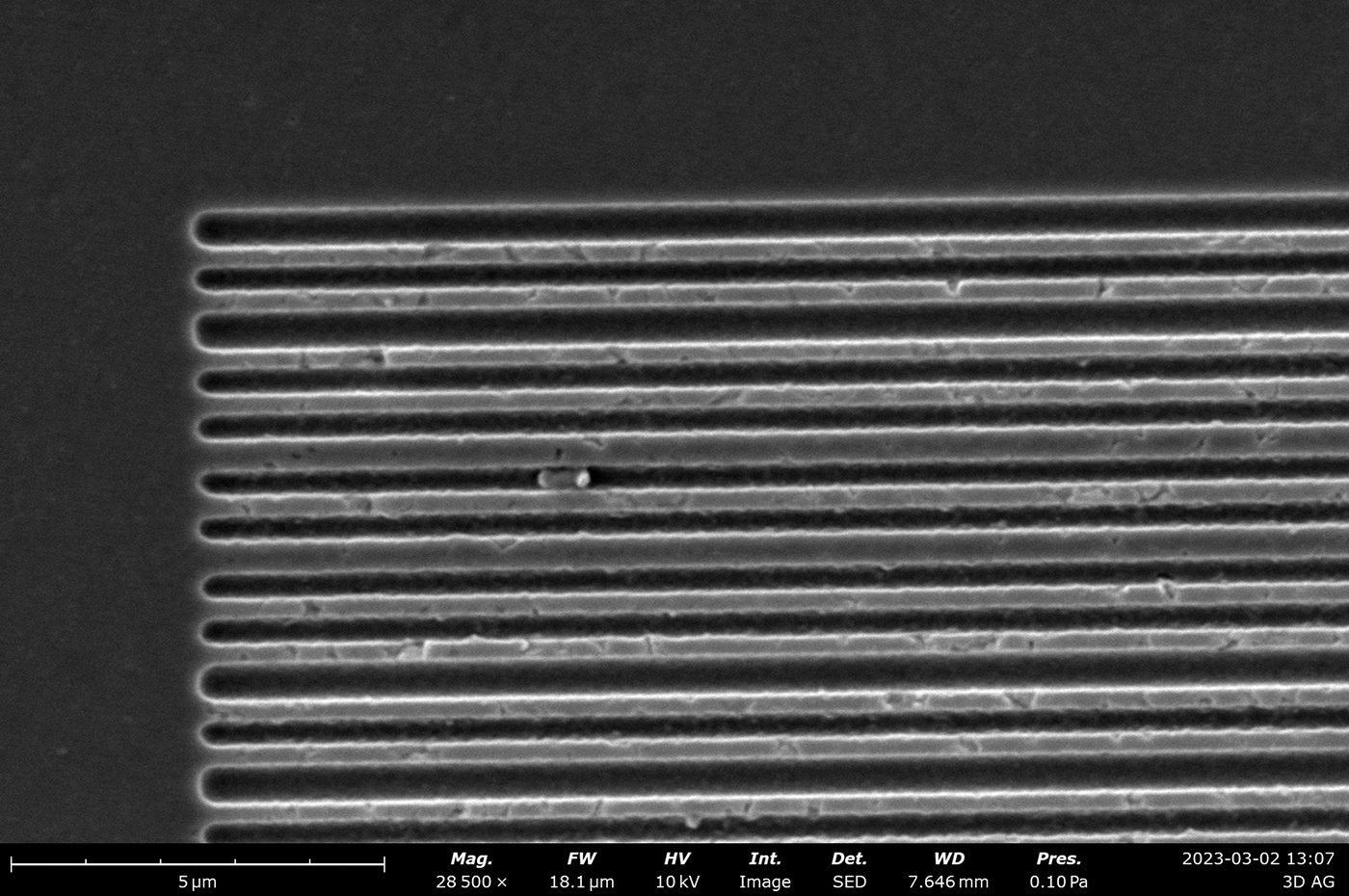
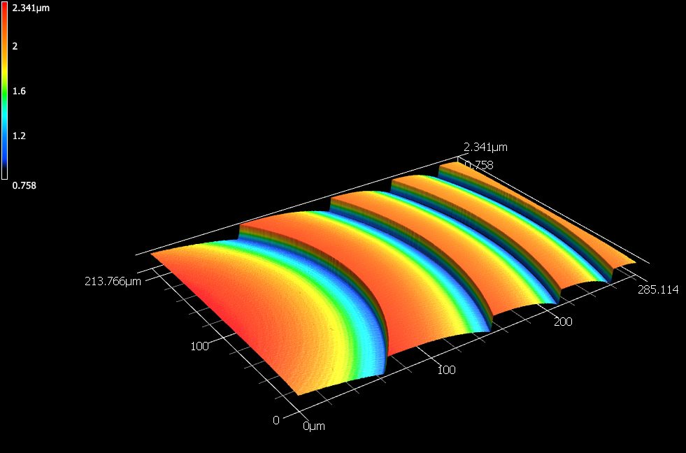
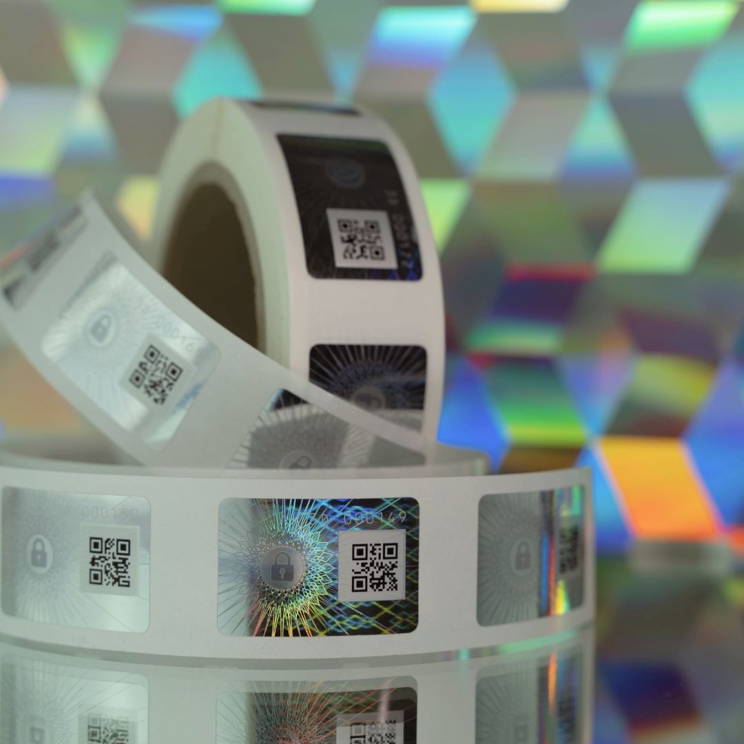
- Holographic / diffractive structures
- Anti-reflection structures
- Aspherical & spherical structures
- Lens arrays
- Gratings (blazed, line, dot)
- Meta structures
- Hydrophobic structures
- Aerodynamic structures
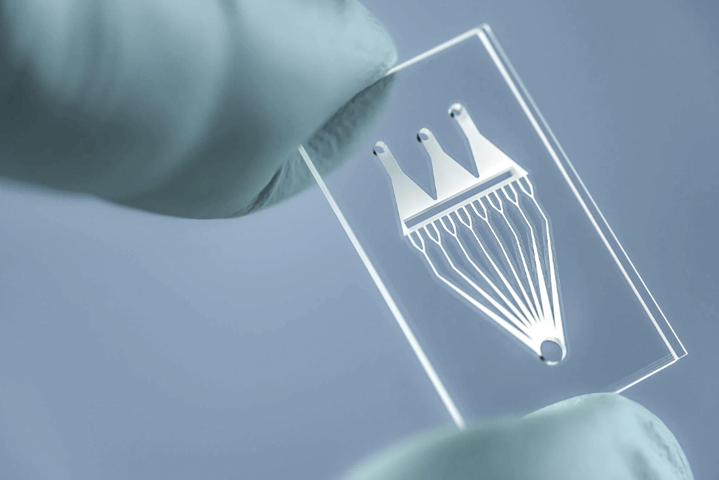
- Microfluidics
Engineering Solutions for Nanostructured Materials:
Identifying Optimal Mastering and Nanopatterning Techniques
At 3D AG, we understand the critical role that mastering and nanopatterning techniques play in the creation of high-quality nanostructured materials. That's why we offer expert support to help you identify the optimal approach for your unique project needs, from the initial lab stage to the final product. Whether you're working on a breakthrough technology or need to improve an existing process, our team of skilled professionals is here to help you achieve your goals with precision, efficiency, and excellence.

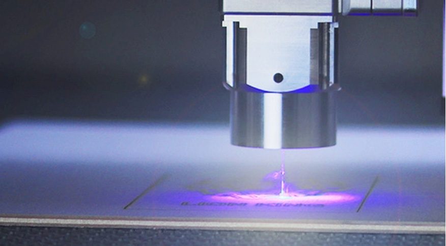
Established Micro and Nanofabrication Techniques
The design of a specific nano and microstructure, its engineering tolerances, expected roughness and many other factors will define which fabrication method is suitable. The existing micro and nanofabrication techniques cover the broad range of dimensions from the micron to the nanometer scale, each technique with its own benefits and advantages, as well as limitations. The following overview lists the most commonly used techniques, all of which 3D AG works with on a regular basis.
- UV Lithography
- Direct Laser Writing
- e-Beam Lithography
- Laser Interference Lithography
- Nanoimprint Lithography (NIL)
- Photopolymerization
- Laser Ablation & Etching
- Micromachining & Diamond Turning
3D Insights


Get in touch
Laettichstrasse 4a,
6340 Baar, Switzerland
You need to load content from reCAPTCHA to submit the form. Please note that doing so will share data with third-party providers.
More Information