PhotonicsViews: Nickel Shims with Large-Format Gratings Originated by Diode Laser-Driven Interference Lithography
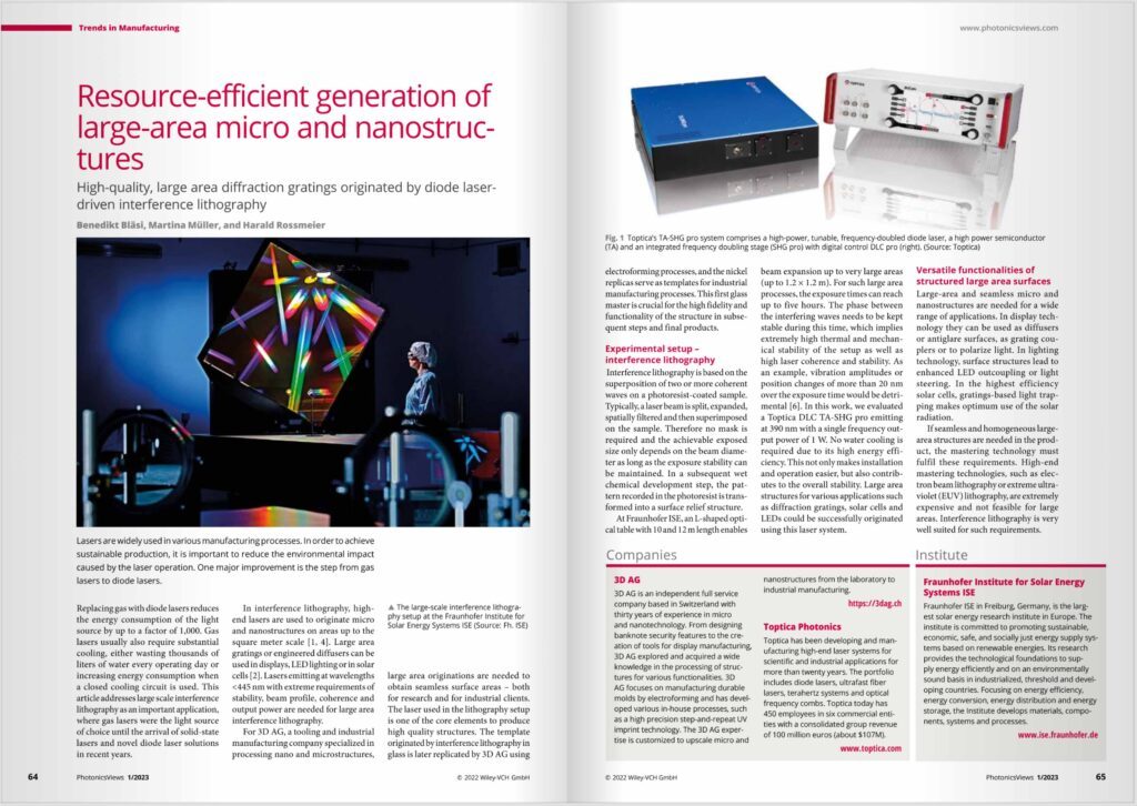
The Fraunhofer Institute for Solar Energy Systems ISE, Toptica Photonics, and 3D AG have published a joint application note describing the benefits of diode-laser interference lithography, the connected manufacturing steps, and the commercial need to produce high-quality and large-area diffraction gratings. The paper, published in PhotonicsViews, focuses on describing various processes involved in product integration and the importance of reducing the environmental impact of lasers in manufacturing environments.
Interference Lithography for Versatile Functionalities of Large-Area Surfaces.
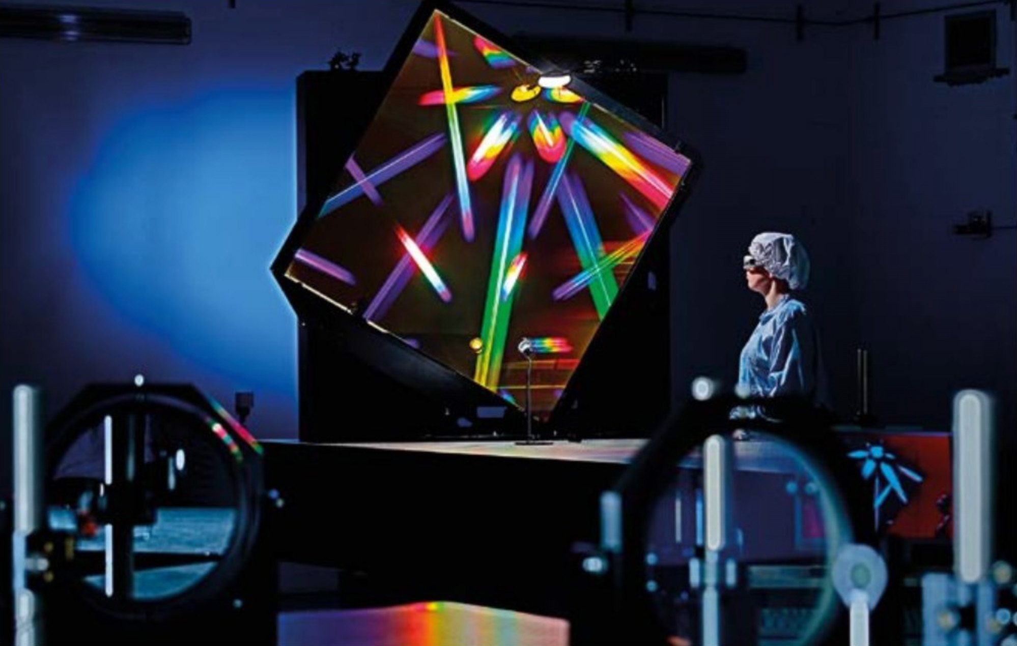
Interference Lithography is based on the superposition of two or more coherent waves on a photoresist-coated sample, with the achievable exposed size dependent on the beam diameter. In this paper, we describe the setup at Fraunhofer ISE, which includes a 12m optical table capable of handling substrates up to 1.2m x 1.2m in size.
One of 3D AG’s core competencies is upscaling and the development of tools for large-format manufacturing of functional structures, such as display or solar masters. As an industrial partner, 3D AG emphasizes the advantages of using diode lasers in the Fraunhofer lab from a commercial perspective. Additionally, we outline the process steps of metal deposition and electroforming, which are essential in creating the final tool.
Resource-Efficient Generation for Environmental Impact of laser Manufacturing.
Replacing gas with a diode laser significantly reduces the environmental impact of laser manufacturing. Toptica Photonics has been developing and manufacturing high-end laser systems for 20 years. The benefits of diode lasers and their capabilities are discussed and summarized in the application note.


